EDA Confidential ...
___________________________________________________________
EDA360: the way forward
by Peggy Aycinena
___________________________________________________________
February 9, 2011
While attending the Common Platform Technology Forum on January 18th in Santa Clara, I ran into an EDA guy in the Exhibit Hall that I've know for a long time – a really seasoned veteran of the industry. Gesturing over towards the Cadence booth nearby, I asked him what he thought of EDA360.
To my astonishment, he asked, “What's EDA360?”
“Oh my gosh,” I said. “You haven't heard of EDA360? Where on earth have you been for the last 9 months?”
******************************
The When of EDA360 …
It's been just under 300 days since Cadence's highly touted EDA360 debuted at a big, splashy event on April 27, 2010 at the Tech Museum in San Jose. The evening's agenda included an hour-long Press Conference with Cadence CMO John Bruggeman, complete with yummy food and a bound copy of the 30+ page EDA360 manifesto.
Following that, there was a highly choreographed show on the Big Stage in the Museum's IMAX theater with performances from Cadence CEO Lip-Bu Tan, [now] Coverity VP Andreas Kuehlmann [waving around a first-edition copy of Mead/Conway's Intro to VLSI Systems], Nvidia's Director of Hardware Engineering Narendra Konda, Wind River CSO Vincent Rerolle, Cadence SVP Nimish Modi, and of course, John Bruggeman, who described the evening as a “truly seminal event.”
After the IMAX pyrotechnics, there was yet more [yummy] food and wine, and a chance to get up close and personal with the also-just-announced Palladium XP simulation-acceleration-emulation verification box. All told, the evening was a tsunami of sensory overload, and quite the glam kick-off for something that – in the days following the event – was greeted with no small amount of skepticism from the EDA industry.
Cadence's EDA360 was not heralded as the Next Coming, despite the fun, food, and frolics of April 27th. But now, almost 10 months into its saga, EDA360 and its evangelists may be enjoying a bit of revenge at the expense of their colleagues/critics – the kind of revenge that's best served up cold.
******************************
The Why of EDA360 …
Per everything I've read and heard about EDA360 over the last 9+ months, the concept was developed by Cadence to “Counter The Semiconductor Industry's Greatest Threat!”
That's a pretty tall order, since not all of you might agree which particular threat – among the many – constitutes the Greatest Threat.
Nonetheless, per EDA360 evangelists at Cadence, “The EDA industry now stands at a crossroads where it must change in order to continue as a successful, independent market. Without this change, EDA will struggle to solve the increasingly complex problems customers are facing now and in the future.”
Hmm, still a little unclear? Then listen to what John Bruggeman said on a phone call I had with him on May 13, 2010 – the day Cadence announced the purchase of Denali.
Per Bruggeman: “Yes, the Denali purchase is splashy news in the industry, and it's igniting buzz around Cadence as well, but it was not our intention to make splashy news. It was purely done as a fulfillment of the promise we made 2 weeks ago when we launched the EDA360 Vision.
“With that launch, we put a pretty provocative set of thoughts out in the marketplace. We said the design model would be turned on its head by EDA360, would be top-down, driven by applications needs, and would provide greater emphasis on system development.
“With EDA360, we're asking: How can you model system behavior, so that applications development can take place faster and earlier? We're calling it EDA360, because it's a much bigger vision than EDA traditionally has had – now it starts at the system level. What came first, however, was not EDA360 or any particular M&A. What came first was the customer.
“We've all talked a lot about the iPhone and Android, but these are just examples of trends. More importantly, consider that Intel acquired Wind River [July 2009] to provide a more holistic hardware/software solution, Cavium Networks acquired MonteVista [November 2009], and Oracle acquired Sun [April 2009].
“So, what came first – even before publishing EDA360 – was a tsunami of partner maneuvers in the marketplace, at our customers, and at our customers' customers. Yet, most of the EDA industry sat on its hands and didn't respond. Cadence, however, held up their hands and said, 'We'll respond!'
“EDA must do much more than it does today! We must make a major move into SoC realization. I think all of EDA is in transition, or had better get into transition. If EDA were to remain on its current path of these little incremental or iterative advancements, there can be many different outcomes, but not one of them would be favorable to EDA. So, we've given the industry a plan by responding to what customers are telling us.
“And yes, I understand that other people in the EDA industry have been critical of the plan – saying EDA360 is not groundbreaking or earth shattering. But the fact is that we've written it down in a clear and articulate way, and described exactly what the industry needs to do. That will [silence our critics] when they come to understand that we all need to be moving in this direction.
“The days of EDA playing a shell game, particularly in a shrinking market, is not healthy for any of us. If we all are working to grow our market, however, then more power to us all.
“Meanwhile, the other [players in EDA] should know they had better get their track shoes on, and get ready to go. They're going to have to work hard to keep up with Cadence!”
******************************
The What of EDA360 …
If you really follow EDA, you've probably heard something about EDA360 over the last 9+ months, as a lot has been said and written. I decided, however, that rather than read what everybody else has said about it, or quote from various Cadence presentations, I would study two White Papers that the company says are based on the EDA360 vision ...
* “Silicon Realization: A New Approach to Faster, Better & More Profitable Silicon” [Oct 2010]
* “3D ICs with TSVs: Design Challenges and Requirements” [March 2010]
In so doing, I've extracted from these texts several Boring/Bad triplets that Cadence says characterize a mis-guided adherence to Traditional EDA ...
* Just more Place&Route – More efficient op-amps – Merely speedier tools
* Just more Iterative – Just more Sequential – Just more Point Tools
* Increased indirect Costs – Class Action Suits – Implications to Brand
Meanwhile, here are the Good/Great triplets that Cadence says will result from embracing EDA360 ...
* Semiconductor Co's – IP Providers – Foundries
* System Realization – SoC Realization – Silicon Realization
* Faster – Better – More Profitable
* Broader – More Efficient – More Effective
* Create – Integrate – Optimize
* Design – Implementation – Verification
* Verification – SiP/Co-Design – Global Productivity & Metrics
* Deterministic – Interoperable – End-to-End
* Intent – Abstraction – Convergence
* Functionality – Electrical Specifications – Physical Requirements
* Analog – Digital – Mixed-signal
* Mixed-signal – Low Power – Giga-Gates/GHz
* Analog/Digital IP – SoC subsystem/complete IC – Package
* Productivity – Predictability – Profitability
So, where does all of this leave us? Do we better understand what EDA360 is from reading through these lists? I don't think so.
Instead, let's read from the original EDA360 manifesto/vision document/mission statement distributed at the launch party last April. [You can download your own copy of the PDF from the Cadence site, although first you have to register.]
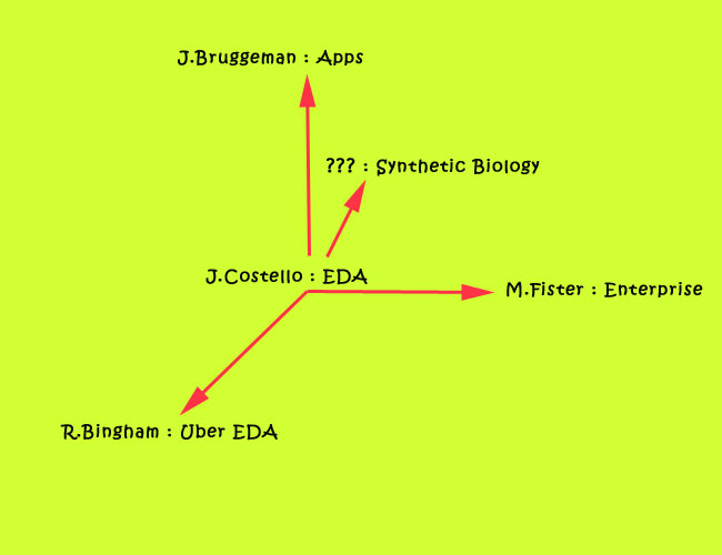
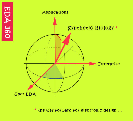
With EDA360, users start with an understanding of the software applications that will run on a given hardware/software platform, define systems requirements, and then work their way down to hardware and software IP creation and integration.
EDA360 includes System Realization: the development of a complete hardware/software platform that will provide all necessary support for end-user applications.
EDA360 includes SoC Realization: the completion of an individual SoC (or alternative packaging choices such as 3D ICs).
EDA360 includes Silicon Realization: represents everything that it takes to get a design into silicon, whether that be an analog or digital IP block, an IP subsystem, or a complete IC without embedded software.
Meanwhile, and in case you're still not getting it, let's go back to the Silicon Realization White paper mentioned earlier …
“Silicon today must be designed with software in mind, not just thrown “over the wall” to firmware, OS, and application developers. Success and profitability will come only with a strong focus on the end product and the applications that silicon will enable.”
In other words – if I'm reading all of this correctly – EDA360 is about looking at the overall system specifications for a product, and then moving down various levels of abstraction until each team involved knows what they need to do to create something that will seamlessly integrate back up into the finished product.
In other words – again, if I'm reading it correctly – EDA360 is ESL. It's pretty much that simple, which brings us to the next topic.
******************************
The Who of EDA360 …
John Bruggeman, a true EDA360 zealot, has proven to be the ultimate WMD for Cadence in promoting the EDA360 franchise.
He was everywhere last spring during the debut and initial dog-n-pony show[s] associated with EDA360. He was a highly visible presence at DAC 2010 – in the Cadence booth in the Exhibition Hall, on stage at the Denali party, and participating in various panels at the conference. He was on stage this past November with ARM EVP Simon Segars at ARM Techcon, and was mentioned proudly by Cadence CEO Lip-Bu Tan during the January 2011 EDAC CEO Vision panel in San Jose.
EDAC panel moderator, Dan Nenni, gently kidded Tan about the famously evangelical nature of Bruggeman's EDA360 pitch, but the Cadence CEO would have none of it. Instead, Tan graciously noted that it was clear the other EDA companies in the room envied Cadence their Chief Marketing Officer, and that was the way it would stay.
When I met with Bruggeman and Cadence VP of Corporate Communications Lynn Cox last June at DAC in Anaheim, Cox told me at the outset of our hour-long discussion, that EDA360 had emerged out of a monastic week of solitary confinement for Bruggeman back in 2009 when – shortly after joining the company – he shut himself into his office at Cadence, experienced some sort of epiphany, and emerged at the end of that week having covered his white board with runes and ruminations, which – like great stone tablets of yore – constituted the EDA360 revelation and a roadmap for Cadence, the larger EDA industry, and the entire semiconductor supply chain. Lynn Cox said Bruggeman's EDA360 insights were nothing short of historic.
And, by the way – if you think I'm kidding about the profound and reverential nature of the way this story was told to me, think again. Bruggeman, by DAC 2010, was delivering a Fire-and-Brimstone stump speech out on the speaking circuit that was nothing short of biblical in its scale, emotion-laden in its delivery, and heart-stopping in its dramatic implications and messaging ...
The End is near for EDA! Repent!
******************************
The Where of EDA360 …
Cadence sits within a family of companies that constitute the EDA industry, a series of companies that provide design infrastructure, methodologies, and tools, as well as IP.
Given the claims of EDA360, it's worth asking if Cadence is the only EDA vendor to provide this vision – a complete end-to-end analog and digital design flow, with verification, implementation, IC packaging and PCB solutions that also provides a path for integrating embedded software applications.
* Let's see how Magma Design Automation describes itself …
Magma's EDA software provides the “Fastest Path to Silicon” and enables the world's top chip companies to create high-performance ICs for cellular telephones, electronic games, WiFi, MP3 players, digital video, networking and other electronic applications. Magma products are used in IC implementation, analog/mixed-signal design, analysis, physical verification, circuit simulation and characterization.
* Let's see how Mentor Graphics describes itself …
Mentor Graphics is a leader in electronic design automation. We provide software and hardware design solutions that enable companies to develop better electronic products faster and more cost-effectively. We offer innovative products and solutions that help engineers overcome the design challenges they face in the increasingly complex world of boards and chip design. The Mentor portfolio includes: Aerospace and Military solutions; Automotive Solutions; DO-254 Solutions; Low Power Solutions; and Manufacturing Variability Solutions.
* Let's see how Synopsys describes itself …
Synopsys is a world leader in EDA, supplying the global electronics market with the software, IP, and services used in semiconductor design and manufacturing. Synopsys' comprehensive, integrated portfolio of implementation, verification, IP, manufacturing, and FPGA solutions helps address the key challenges designers and manufacturers face today, such as power and yield management, system-to-silicon verification and time-to-results. These technology-leading solutions help give Synopsys customers a competitive edge in bringing the best products to market quickly while reducing costs and schedule risk.
* Let's see how Tanner EDA describes itself …
Tanner EDA provides a complete line of software solutions that catalyze innovation for the design, layout, and verification of analog and mixed-signal ICs. Customers are creating breakthrough applications in areas such as power management, displays and imaging, automotive, consumer electronics, life sciences, and RF devices. A low learning curve, high interoperability, and a power user interface improve design team productivity and enable a low total cost of ownership. Capability and performance are matched by low support requirements and high support capabilities. as well as an ecosystem of partners that bring advanced capabilities to AMS designs.
* Finally, let's see how Cadence describes itself …
Cadence enables global electronic design innovation and plays an essential role in the creation of today's ICs and electronics. Customers use Cadence software and hardware, methodologies, and services to design and verify advanced semiconductors, consumer electronics, networking and telecommunications equipment, and computer systems.
My point in laying out these many paragraphs of market-speak from these five EDA vendors is two-fold.
* Not one of these companies seems to be panicking, on the edge of despair, or standing “at a crossroads where it must change in order to continue [the EDA industry] as a successful, independent market.”
* Not one of theses companies' blurbs – including Cadence's own market-speak – mentions the burning need to move up several levels of abstraction to focus on an embedded applications point of view, so as to guarantee the impact or validity of the tools these vendors provide for hardware and hardware/software design and verification.
Now, having said that, who's to say that the future of semiconductor hardware does not include the move to a single, vanilla-flavored platform, one that can be tweaked as needed to provide the proper foundation upon which to layer a host of increasingly complex embedded and/or sophisticated apps.
Certainly that vision has always been one near-and-dear to my own heart, but for right now I'm not seeing that as a state-of-the art demand within the hardware part of the semiconductor supply chain – or the EDA vendors who service that part of the market. Things could change, I'm just saying it ain't there yet.
So that's where we are, in my opinion. Of course, Cadence doesn't care about my opinion – nor should they – so their pursuit of the EDA360 vision continues on.
******************************
The How of EDA360 …
The easiest way to see how Cadence has implemented their EDA360 vision is to examine briefly the time line of the last 10+ months. It included, among other things, a full-on industry blitz starting in March 2010 at DVCon, when CEO Lip-Bu Tan gave a broad-reaching keynote address that, in retrospect, was full of EDA360 terminology. Following DVCon, the pace of company news associated with EDA360 sped up ...
April 2010
* EDA360 Launch Event
* Palladium XP announced
May 2010
* Denali Acquisition
* Open Integration Platform announced, “a key pillar in the EDA360 vision … comprises integration-optimized IP from ecosystem participants: Cadence, GDA, IBM, RapidBridge, Sonics”
* Announcements re: DDR Phys, Memory controllers, PCIe, Ethernet protocols
June 2010
* Obvious DAC presence: “Our goal is to be everywhere,” CMO Bruggeman declared.
* Hosts Denali party: Bruggeman promises the party will continue for at least 15 years.
* SOI Design Hub announced
* Additional capabilities announced for TSMC Digital Reference Flow 11.0 & AMS 1.0 at 28 nm
* “Most comprehensive” Open Source Reference Flow supporting UVM announced
August 2010
* Workforce “re-aligned” to match EDA360 Vision
* Named to lead System & SOC Realization R&D – SVP Nimish Modi
* Named to lead Silicon Realization – SVP Chi-Ping Hsu
October 2010
* IP Ecosystem microsite announced to “increase FPGA & ASIC designers' visibility to the latest IP supporting the Xilinx programmable platform ... will be part of ChipEstimate.com”
* “Holistic approach” to Silicon Realization emphasized
November 2010
* EDA360 Vision and Ecosystem demo'd at ARM TechCon
January 2011
* 600+ capabilities in Virtuoso that augment/dovetail with UVM announced
* Qualified 32/28 nm reference flow targeting Common Platform technology announced
* Collaboration with STARC announced to create 32/28nm DFM flow, “aligned with the EDA360 vision”
* Encounter-based flow announced with “faster, more deterministic path to achieve giga-gate/gigaherz silicon”
February & March 2011
* EDA360 Tech on Tour announced with 4 events in North America, 4 in EMEA, 7 in Asia.Meanwhile, in and around all of this, there were announcements of EDA360-aligned customer wins and/or partnerships with VIA Centaur, IBM, Silicon Integrated System, Innofidei, Casio, STMicro. Hitachi, NationZ, Fujitsu, Realtek, ARM, Andes, Global Unichip, SMIC, Sunplus, Open Silicon, Spreadtrum Communications, and Wind River. Some of these announcements also bragged on contributions from Cadence Global Services.
Additionally, CDNLive! – which had withered to a virtual shadow of its former self during Cadence's Dark Times – was resurrected, live and in person, in Silicon Valley and elsewhere.
All in all, it has indeed been nothing short of a blitz of news and notices that has defined the How of EDA 360.
******************************
The Real Why of EDA360 …
Not surprisingly, it's never easy to implement a sea change within an organization, and EDA360 must be viewed as exactly that – a sea change within the Great Ship of State at Cadence. And that's not to say that a Sea Change wasn't warranted.
It's not even close to ancient history that a short 18 months before the April 2010 launch of EDA360, there was a cataclysm of unparalleled proportions at the company as the entire executive team was axed in one swift, surgical blow from the Board of Directors.
SAN JOSE, CA, 15 Oct 2008
Cadence Design Systems, Inc. today announced that its Board of Directors has formed an Interim Office of the Chief Executive to oversee the day-to-day running of the company's operations, effective immediately … [following] Michael Fister's resignation as President, Chief Executive Officer and a director of the company, by mutual agreement … Kevin Bushby has resigned as Executive Vice President – Worldwide Field Operations, effective immediately … the company also announced the resignations of James S. Miller, Jr., Executive Vice President – Products and Technologies Organization, William Porter, Executive Vice President and Chief Administrative Officer, and R.L. Smith McKeithen, Executive Vice President – Corporate Affairs, effective immediately.
The effect of all of this was indeed immediate – further collapse of the company's stock valuation, the swift onset of more than a dozen stock holder lawsuits, and dire predictions from a host of industry observers that Cadence was done, toast, history.
Those prediction, however, turned out to be wrong. In fact, Cadence was not done, toast, or history. Instead, under the leadership of the acting-turned-permanent CEO Lip-Bu Tan, the company rallied over the next 18 months, apparently rebuilt itself from the inside out, went out and hired a hall, and put on a really big show in April 2010 that was not anywhere near as much about announcing EDA360, as it was about announcing that, despite all of the rumors to the contrary, Cadence was back – with a vision and a vengeance.
Now almost 10 months after that show of force at the Tech Museum in San Jose, Cadence is definitely in the fray. So much so, that during Cadence's January 2011 earnings call with The Street, CEO Tan was able to proudly announce, “Thanks to our bold vision, we have aligned our company strategy and operating plans around [the EDA360] vision, and delivered new and impactful technologies, products, and design flows in the 3 areas of System Realization, SoC Realization, and Silicon Realization … [We've] acquired Denali Software, and accelerated our road map in the area of IP.”
Tan went on to brag that the company demonstrated a revenue growth of 10 percent in 2010, year over year, since 2009, “has good customer momentum, especially at the large semiconductor companies, and a strong pipeline of [products underway].”
More succinctly, per the Cadence 2010 earnings Press Release: “Revenue for fiscal 2010 totaled $936 million, compared to revenue of $853 million in fiscal 2009. Net income for fiscal year 2010 was $142 million … compared to a net loss of $150 million for fiscal year 2009.”
There was also ink in the announcement noting additional good had resulted from settling an “IRS examination of Cadence's federal income tax returns for the tax years 2000 through 2002, and a $67 million acquisition-related income tax benefit.”
But most importantly, the Press Release said, “For the full year 2011, the company expects total revenue in the range of $1,030 million to $1,070 million.” [Yes, more than a billion dollars!]
Yeah, it's true that all of these are non-GAAP numbers, but that's not the point The point is that the Real Why of EDA360 has almost nothing to do with the larger EDA industry – or the even larger semiconductor supply chain. Instead, it has everything to do with a rallying cry, a unifying vision, and a renewed sense of pride within the Cadence organization itself.
EDA360 can, as mentioned above, be read as “ESL” by those outside of the company. But for those inside of the company – particularly those who have survived these last several years of way, way downs and way, way back ups – my guess is that EDA360 can be read quite simply as ...
“Go Team!”
*******************************************************
The way forward for electronic design …
___________________________________________________________
Peggy Aycinena owns and operates EDA Confidential:
www.aycinena.com
Copyright (c) 2011, Peggy Aycinena. All rights reserved.