Design for Manufacturing:
The Foundry's Point of View
An interview with Walter Ng ...
by Peggy Aycinena
May 29, 2006
*********************************************
Walter Ng, Senior Director for Design Solutions at Chartered Semiconductor, is a man on a mission. He wants people to understand the role foundries are playing in building design platforms to address the design-for-manufacturing conundrum facing the semiconductor supply chain in the deep-submicron era.
Given the widespread concern regarding the manufacturability of complex designs under development today, it was great to be able to speak with Walter about DFM. It was also great to pose some of the same questions to Walter Ng that Blaze DFM CTO Andrew Kahng had answered earlier this month.
If Andrew's responses are representative of the EDA community and Walter's representative of the manufacturing community, I think the two interviews together provide a detailed and important overview of where we stand as we head into mid-2006 and the run-up to the Design Automation Conference in San Francisco in July.
*********************************************
DFM Clarified ...
Q – Who needs to care about the definition of a DFM tool? EDA tool providers? Designers? Mask makers? Equipment vendors? Manufacturers?
Walter Ng – I think right now, when we’re talking about the problems of today, the two partners in DFM are principally the EDA tool providers plus the manufacturers. For the others – the designers, mask makers, and equipment vendors – there are longer cycles and lead times for change. What’s there today, in terms of equipment and mask technology, is there.
People could be looking at ways to improve some of the mask-equipment technology – and hopefully those guys are looking at the next technology node – but to fix and address the problems we’re seeing today, it’s really an issue for the design tool vendors and the manufacturers. That’s why we’re working aggressively on the platform with those folks.
There’s been criticism in the press about the foundries and their unwillingness to work with the EDA vendors, but for those of us working on the platform, the walls are definitely coming down. We’ve been working very closely with the EDA tool providers. They have received a good amount of data from us to help them create and enhance the tools, and things are definitely moving forward in an optimistic way.
Last year, after the platform was announced, we were surprised that one of the editors in the industry was very critical of what we were doing with our DFM initiative. We were actually a little shocked about that one write-up, in fact, because we knew the real inside story of how we were, and are, working with some of the our EDA partners.
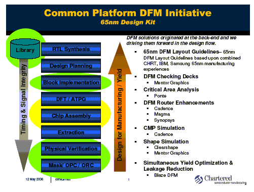
A couple of weeks ago, we released our 65-nanometer offering in the DFM space for the platform. We are hopeful that people will fully understand and recognize the kind of cooperation required between all of the players involved to develop this type of announcement.
[Editor's Note: Chartered Semiconductor has partnered with IBM and Samsung on the DFM platform Walter references here. For more information about that collaborative effort, please see the website.]
Q – At what specific process technology node did the need for a DFM flow emerge?
Walter Ng – It’s funny, but I still don’t believe that everybody has a common definition for DFM – it’s such a broad term. Some folks, for instance, would say, "Well, we’ve been doing DFM for as long as there have been DRC packs. DFM is distinguished by what can support manufacturing, and what cannot."
So, you could say that all the way back to the early process technologies, there has been some form of DFM. But, what’s happened over time, and what has certainly renewed the focus on doing more DFM, is that the things we had been doing were beginning to be insufficient.
That situation really began to develop at 0.13 micron, particularly on the manufacturing side. We began taking a much more hands-on approach to working with our library partners, and much more hands-on approach with the EDA folks at 0.13 micron.
That was really the technology node, and each one after that, where it was expected that additional effort was going to be needed to improve what we had put in place up to that point, to keep up with what we had been doing previously in manufacturing.
Q – What generic tools are needed in a DFM flow?
Walter Ng – DFM tools are an elusive animal. There are multiple, different problems so the answer to the question is always, "It depends on what you’re trying to focus on."
DFM tools help resolve problems in a variety of areas. If it’s a random defect problem, it’s different than a systematic problem. From our standpoint, we’ve identified a certain set of capabilities that we believe arm the designer with the appropriate capabilities for the appropriate problem.
The main focus of our platform initiative is to drive a correct-by-construction approach. We’ve qualified the tools in the platform, and now have put in support for capabilities that allow designers, plus their design-chain partners, to build good, base elements.
For instance, at the standard cell level, at the lower foundation level of design, if those pieces are manufacturing-friendly, those are the pieces that get replicated again and again. They will be much improved over the lifetime of the product through critical area analysis [CAA].
CAA is a model-based approach to identifying possible hot-spot areas in the design at the cell level. We augment CAA with a rules-based approach, which is what we have in our DFM checking-decks – a set of rules that give designers some guidelines. So, ours is a rules-based plus a models-based approach.
In addition, we also are using litho-simulation and shape simulation to try to make sure, from an OPC and RET standpoint, that the design will be printable with a high degree of confidence and a high yield. Those are the pieces at the lower level that we feel are important with respect to making sure the foundation pieces are good.
Now, later in the design flow, your chip is more or less fully implementable, so designers are less prone to be willing to makes changes. Again, what you're talking about here is placement and routing, and what we're driving is in conjunction with the major companies in the implementation space – Cadence, Synopsys, and Magma. We're working on implementations and routing down in a correct-by-construction manner for manufacturing.
If we have enabled our tools to do the right thing at the foundation level, and have worked [successfully] with the Big Three on their tools to drive more correct-by-construction at the implementation level – then, at the end of the day, the chip will have a good amount of manufacturing awareness.
That's the philosophy that we've taken in our common platform and in our DFM approach. There will be statistical timing analysis [STA] – or what I would rather call, "variation-aware timing."
That's about trying to model from the manufacturing side, and working with the EDA vendors to model sources of dominant variation in the manufacturing process – then, using those models in the right way to allow timing analysis and validation.
Q – So, it sounds like we're in good shape at this point.
Walter Ng – Well, we're making progress in the STA space, but there's work to be done in the litho-aware space – further refinements could be done. At the point where the base technologies are available, they could be improved, but improvements are coming as we work more closely with the EDA industry.
Q – What's the short list of physical effects that necessitate resorting to DFM tools?
Walter Ng – From a timing standpoint, we're really looking at the systematic issues that cause variation, and we're certainly looking at capturing some of the random defects.
Up front, when a process just becomes available, part of what most people feel they're looking for in DFM capabilities is related to the question, "How I make my design friendly to what's called manufacturability?"
Q – Are those things important just for early adopters of a technology node?
Walter Ng – No, it's not just for early adopter. But as a process node becomes more and more mature, a lot of systematic issues tend to get wrung out. We're getting there at 90 nanometers. A lot of the systematic problems have been wrung out, so some of the toolkit capabilities should be either very well understood at this point, or the necessity for them may not be as great, so that may not be the place where continued focus should be put. After a process becomes more mature, it's more the random part of the defect that causes problems.
The other main area of concern is with regards to lithography. People have been doing OPC and RET, and all that DFM consists of there. As we go to smaller and smaller geometries, shorts and opens and interactions at that very low level are much more of a concern.
In broad categories, the physical issues we're trying to address are to model and capture the variations in the manufacturing with regards to some of these failure mechanisms – and then on the back-end, OPC, RET, lithography and shape are the kinds of issues.
The other class of effects is very much related – metal density and the issues that come along with bond uniform metal density. Again here, we're trying to push for correct-by-construction.
So, there are 2 issues as you do the physical implementation and look at routing on each metal area. Is routing done that's creating a lot of hot spots, or is it fairly well placed out in a distributed manner? If it's not, then on top of that, how do you insure better metal fill, so the combination of routed metal and added metal produces the uniformity that you want to get?
It's really these types of issues that impact directly on the parasitics, with relation to the interconnects and signal integrity and timing analysis. There's a lot involved and a number of different tools, as you can see in our solution that we've made available in the platform.
We've taken an approach where we've formed teams on the common platform. In each one of these different kinds of areas, we've put together the best folks in each company – various committees on design guidelines. DFM checking deck, the reference flows, litho- and shape-checking areas, variation-aware timing, and critical timing analysis. These are all submicron issues.
Samsung, Chartered, and IBM – we've taken the best of breed, and gone out and evaluated tools that are commercially available, and selected what tools are the best in each of these areas.
Then, whatever tools that is – that's the partner we've begun working with in each individual space. It helps to drive the technology and the tools in the direction that we commonly believe it needs to go in. There partners are like Mentor and the Big Three – Synopsys, Cadence, and Magma – plus some smaller folks as well including Ponte, Clear Shape, as well as some start-ups that have since been acquired.
We're looking at where we think is the most competitive tools that will help our designers, enabling them to help themselves. If the necessary data is available in these tools, our goal really is to get the designers to use these tools – not to feed the designs into Chartered and then we run the tools.
We could do that, of course – and have done that already at times as a service – but we also want to make sure that for those customers who want to do it themselves, we can allow them to do it.
There's a caveat, of course. In some cases, it may be like giving someone a loaded gun. Because, what we see is a wide spectrum of customers.
There are big guys driving 65-nanometer designs. They typically have large teams of folks and want to do things themselves. They very product literate and understand products and design. These types of leading-edge guys don't want services – it's just not appropriate. Within the turn-around time they design in, they can't be waiting on anybody else to give them feedback.
The next kind of guys are a mixture of both – fast followers, who are somewhat like the lead guys, but don't have all the process expertise in-house. Then there are the smaller guys and late followers. They will tend to rely more on a services model. Of course, there's nothing wrong with either approach. With the platform, we acknowledge the need to enable all types of customers.
Q – Distinguish between DFM and DFY, or are those concepts a continuum?
Walter Ng – DFM is really about trying to drive practices that allow a design to be more manufacturable. That's what we're doing in the parts of the solutions that we're enabling. So, when we put out a recommended-rule deck, the rules in there help designers understand what the guidelines are around making a design manufacturable.
For DFY, however, there are other capabilities in the tools that say how much more manufacturing-friendly you're going to be, how to make your design as high yielding as possible.
We see the difference between DFM and DFY as the difference between something that's manufacturable and something that may take additional effort on the back end to make it high yielding.
DFY is usually about trade-off issues. It could be as simple as increasing spacing [in the design] under certain circumstances. In creating interconnects in the layout, you can certainly increase spacing and that will ensure a higher yield. However, if you're willing to take a chance on less initial yield for a more compact layout, [you can make that choice as well].
Q – So how does DFT fit into that continuum?
Walter Ng – DFT is a must. Everybody's come to understand that fairly well. DFT is something that most designs have incorporated in one form or fashion, probably since .35 or .25 micron. Today, it's more BIST [built-in self test] than anything – that's the only way to test some of these huge designs.
Q – At least now, there's so much on-chip real estate these days that DFT structures aren't seen as burdensome anymore.
Walter Ng – Actually, from the designer's side, they don't care if more space has been opened up, they're still not going to [happily] give you those test structures.
I started out [my career] in test, but I got out of it. Test, even today in most companies, is seen as a necessary evil. The designers say they'll only dedicate as little real estate as possible to it.
In fact, it's the rare company today that really puts a priority on test, [although] it's better than in the past when test used to be just an afterthought. The main design team would go through and do their design, and then the test engineer would come over and see what needed to be done to test it. You had to bargain and cajole to get the design team to make any changes at all.
Now, testability is recognized as a must, so the test teams are in there with the design teams. But nonetheless, they're still second-class citizens.
Q – Getting back to DFM, when we're down to a dozen or so atomic layers in some modern on-chip structures, is there really any hope of accurately predicting or controlling the outcome of manufacturing aberrations at these geometries?
Walter Ng – I think what we're talking about here is modeling, modeling the possible variations. That's a different approach than trying to predict exactly what some of these issues are.
At these small, small geometries – prediction of exact responses or exact outputs may not be as easy as understanding and modeling what the possible variations in things are. In fact, it serves pretty much the same purposes when we're talking about geometries that are so, so small because the range of variations is very small.
Even with respect to something like lithography, some of the causes of variations are really random, so we can't always have those variations under control. The best way is to provide some kind of measure of possible variation. If you're designing into what that window of "variation-aware" [options], you'll have a very robust design.
At the end of the day, having these additional DFM and DFY capabilities is really going to ensure that when you come out of final design and layout, you'll have a robust design – robust meaning that you understand what these main sources of variation are. The different tools for strategies for design mean you've designed with that understanding. You've made the choices to be manufacturable and still yield within the window of variation.
And that's really what we're trying to drive our customers to do – to build those more robust designs, so that at the end of the day when they tapeout and we've put it into manufacturing, that design will come out silicon right, with a high yield.
Q – Synopsys CTO Raul Camposano gave an address at SPIE where his final slide said, "Synopsys is the only company with a complete DFM solution." What do you think?
Walter Ng – Well, that's a bold statement and, frankly, from the work we've done on the platform our selections of tools are coming from multiple, different partners.
When we evaluated things like critical-area analysis, there was no one company that had all of the solutions in this area, let along the best solution. We just don't see one company having all of the solutions today.
Q – When do we leave CMOS behind, or is it true as Dr. Chenming Hu said at the recent UC Berkeley EECS Research Symposium that the global manufacturing infrastructure is so huge, it is impossible to move beyond it anytime soon?
Walter Ng – If you take a look at the CMOS technologies at 90, 65, and even 45 nanometers, there is more and more technology being thrown into the traditional CMOS – strained silicon, possibly embedded SiGe, and so forth. There are new technologies, plus embedded materials, that continuously need to be developed to prolong the use of CMOS.
I do think there are other technologies out there that certainly can't be ignored, and you should never say never. All companies need to continue to investigate other possibilities. SOI, for instance, is a possibility. The Microsoft Xbox CPU has had a lot of good success with that.
However, if mainstream designs moved onto other types of technology, the design tools and design chain infrastructure would definitely have to be in place to support that move. It depends on what markets are driving the products and continuing to drive the technology down at that level, but certainly CMOS looks like it will continue to have legs for quite some time.
Q – Finally, isn't it the foundries that have the real, complete DFM flow? How can the EDA companies compete, if this is true?
Walter Ng – I want to make a very clear statement here, because a lot of folks may not understand the real situation. I don't believe that there are foundries that are designing EDA tools. [It's a mis-conception] that has to do with the way the solutions are being marketed.
From a marketing perspective, the foundries' market solutions are their own. But, they're really EDA-company standard solutions, enabled by manufacturing and process information from the foundries. That's the traditional model, although some foundries market it in a different way.
Here at Chartered, we're marketing it on a common platform, so we're marketing the DFM solution in a very open way. We've fully named our various partners and are not trying to brand it as our own.
We're saying, "Okay, these are the common platform tools. These are the tools that make up what we suggest as the common platform. They're not our tools!"
Q – Does that put the foundries in a relationship with the EDA vendors that's somewhat of a 'master-slave' relationship?
Walter Ng – This is not a master-slave relationship!
The way I see things in the industry is that EDA companies continue to be masters in tool development, while more and more, we in the foundries are working to address some of the manufacturing issues and try to bring those issues into the design flow.
Clearly, the EDA vendors do need to rely on the manufacturers – and that's not just foundries – for a lot of the additional knowledge that needs to be built into the tools.
This is all very linked to the evolution of the foundries and the foundry model, starting at .35 micron. Foundries don't have our own products or our own design teams, per se, that are doing designs on a daily basis. And certainly, we're not delivering products to the end markets.
Foundries are primarily manufacturing companies, but we don't have a lot of credibility if what we're doing is done in isolation. So what we're saying is, "Here are the design tools for doing such and such."
We believe we are [presenting] a very different model in putting together the common platform. Chartered is strictly a manufacturer, but our partners on the platform – including Samsung and IBM –are very well known, with high competence in the design space.
That mix of a strong manufacturing background and the long history of design expertise all come into play when we're talking about what are the right solutions for DFM and what makes sense in the design environment. The solution needs both competencies.
The foundry model has been evolving. The foundries, alone, can't provide the answers. The common platform model really speaks to something that makes sense – for the foundries, the tool providers, and the designers.
************************************************
May 29, 2006
Peggy Aycinena owns and operates EDA Confidential. She can be reached at peggy@aycinena.com
Copyright (c) 2006, Peggy Aycinena. All rights reserved.